

How Custom EMI Shields Improve Signal Integrity in Dense PCB Designs
2026-11-21
Modern PCBs are shrinking while clock speeds and component counts keep climbing, and that combination turns electromagnetic interference from a minor nuisance into a real design risk. The usual shields may fit the board, but they often fail to keep pace with tighter layouts, split ground planes, or mixed-signal sections. Custom EMI shields change that equation by working with the actual geometry and noise profile of a dense design, not against it. At BOSI, we see how a shield shaped for the exact cavity, venting pattern, and grounding points can do more than contain emissions: it can clean up signal return paths and prevent the crosstalk that standard off-the-shelf covers tend to miss. In this article, we’ll break down where conventional shielding falls short and how custom solutions help preserve signal integrity when there is no room for error.
The Unseen Noise Problem in Tight PCB Layouts
A dense mixed-signal board rarely gives obvious clues about where interference begins. The copper looks clean, the schematic checks out, and the design rules pass, yet the prototype still behaves unpredictably. In many cases the culprit is not a single bad component but the physical arrangement of return currents, vias, and split reference planes. When traces are packed together to save space, the electromagnetic fields they generate overlap in ways that are almost impossible to spot from a layout view alone. This is what makes the noise problem unseen: it lives in the spaces between signals, not in any visible defect.
Tight layouts force currents to find whatever return path they can, even if that path winds through unrelated circuitry. A fast digital line crossing a gap in a ground plane will inject displacement current into nearby analog traces, creating a subtle but persistent offset that drifts with temperature and load. The usual fix of adding more decoupling capacitors often fails here because the issue is not supply ripple but shared impedance in the reference structure. Engineers tend to chase the symptom, swapping parts and adjusting firmware, while the real cause remains buried in the stack-up and via placement.
Even experienced designers overlook how much a small change in clearance or layer assignment can shift field coupling. Two traces that look acceptably separated on screen may still share a slice of dielectric where electric field lines concentrate. Once the board is fabricated, measuring this kind of coupling is difficult without cutting traces or using near-field probes at very specific locations. The most practical defence is to treat every return path as a first-class signal, not an afterthought. That means reviewing where current actually flows, keeping sensitive nodes away from high dV/dt edges, and accepting that on a truly tight board, silence is designed in rather than discovered later.
Standard Shields Leave Gaps Where It Matters
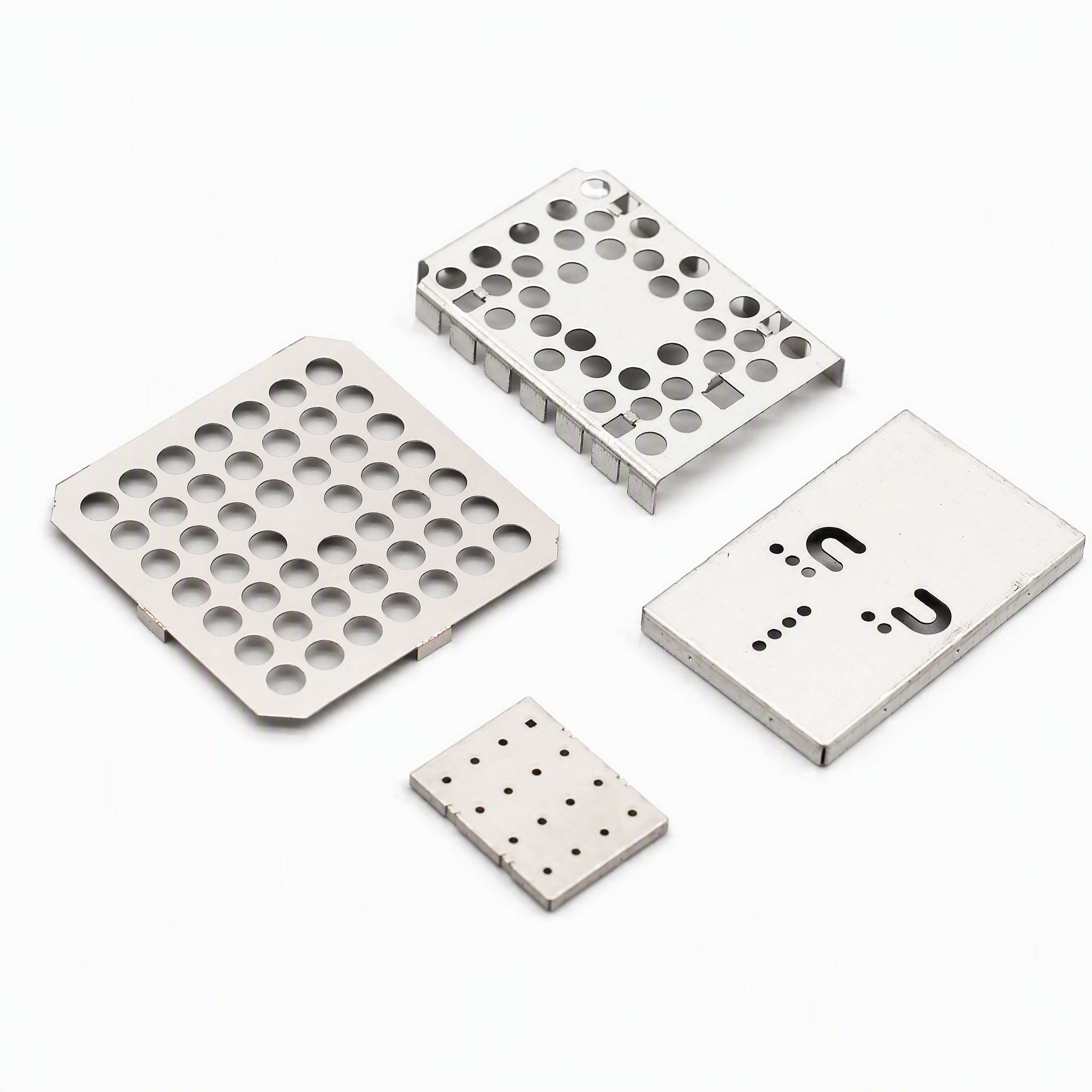
Most off-the-shelf protection looks solid on paper but leaves the edges exposed. The gaps rarely show up in routine checks because they sit where assumptions overlap—between vendor promises, default settings, and outdated threat models. Once an attacker stops following the expected path, those quiet seams become the whole game.
The problem is less about missing features and more about misplaced confidence. Teams patch known weaknesses, tighten obvious entry points, and still leave the less obvious intersections unattended. Those are the places where identity boundaries blur, where one system trusts another without asking twice, and where a small misconfiguration goes unnoticed for months.
Closing those gaps means looking past the shield itself. It helps to trace what actually connects to what, question inherited permissions, and treat every handoff as a possible weak spot instead of a routine step. That is where standard coverage ends and actual resilience begins.
Shaping a Shield Around Real Signal Behavior
Real signal behavior rarely moves in clean straight lines. It stutters, repeats, drifts, and occasionally goes quiet before surging again. Building a shield around it starts with accepting irregularity as normal rather than treating every deviation as a threat. When the baseline is allowed to breathe, the moments that genuinely don't belong begin to separate themselves from ordinary noise.
That separation depends on watching how patterns unfold over time instead of freezing them into fixed thresholds. A burst of activity on a Tuesday morning might be routine for one context and anomalous in another. By weighting recency, sequence, and rhythm together, the shield becomes less of a brittle wall and more of a flexible membrane: close enough to catch distortion, porous enough to let authentic fluctuations through.
The goal is not to sanitize the signal until it looks perfect. It is to preserve the ragged edges that make behavior recognizable while filtering out the pressure that tries to mimic it. A shield shaped this way does not hide real activity behind false calm. It gives the underlying pattern enough room to move without losing the boundary that keeps manipulation out.
Grounding Choices That Quiet Return Currents
Return currents are often treated as an afterthought, but the route they take can make or break a board. When a signal changes state, the same charge that travels down the trace has to find its way back to the source. If that reverse path is forced around a gap in a plane, a connector field, or a poorly placed via, the loop area grows and the circuit begins to radiate or couple into nearby traces. The quietest designs do not leave this to chance; they shape the return path just as carefully as the signal path.
One practical choice is to avoid slots, moats, and long splits in reference planes directly under fast edges. Where a return current hits a discontinuity, it spreads out, raises local field strength, and turns a quiet copper pour into an antenna. A better move is to keep high-speed signals over a single unbroken reference for the entire length, or, if the signal must cross a split, place a stitching capacitor close to the crossing so the return has a low-impedance bridge. That small placement decision often quiets a noisy rail more than an extra decoupling capacitor.
Grounding strategy also matters at low frequencies, where currents favor resistance rather than inductance. A star ground can work well for precision analog sections because it keeps power-stage currents away from sensitive nodes, but it can fail badly if fast digital returns are forced through the same narrow point. Mixed-signal boards often benefit from a single solid ground plane with careful component placement instead of a hard partition. The goal is not a perfect schematic ground symbol; it is giving every return current a short, predictable route home.
Keeping Heat From Becoming the Trade-Off
Thermal management often gets treated as a tax on design: add a bigger heatsink, throttle the load, or accept a thicker chassis. The assumption is that pushing performance means paying with heat. That equation starts to fall apart when the thermal path is treated as part of the product, not a patch applied after the fact. Materials with higher conductivity, shorter interfaces, and shapes that move energy away from concentrated zones change what the system can sustain before it derates.
The real shift happens when heat is no longer framed as waste. It can be directed, spread, or even reused in ways that keep the user experience intact. Instead of a fan ramping up as a last resort, the design moves energy steadily and quietly across a larger surface. The result is less about managing a problem and more about keeping the trade-off from showing up in daily use.
What Changes in Eye Diagrams and Error Rates
A clean eye diagram rarely survives contact with a real channel. As reflections, crosstalk, and impedance discontinuities accumulate, the once-open eye begins to narrow. The crossing point drifts, the rise and fall slopes flatten, and the available timing margin shrinks. What was originally a wide hexagonal opening turns into a sliver, then closes altogether. Error rates follow that same trajectory, but not always in a linear way. A small reduction in eye height can push the receiver past its decision threshold and produce a sudden burst of bit errors.
Jitter is usually the first visible change. Edges start to smear, creating a thicker horizontal spread at the crossing region. On its own, modest jitter may only reduce margin, but combined with vertical noise it forces the sampler to make decisions closer to the signal's uncertain middle. This is where bathtub curves steepen and the bit error rate climbs from ten to the minus twelve toward ten to the minus nine or worse. The eye diagram does not have to close completely for errors to become unacceptable; it only has to shrink enough that the receiver's keep-out region is violated.
Temperature, voltage drift, and aging tend to accelerate these changes. Margins that looked comfortable on a bench measurement erode once the link runs at full data rate with realistic termination, package parasitics, and adjacent lanes switching. Watching the eye collapse in real time is a useful warning because error counters often lag behind the physical degradation. By the time the BER reading spikes, the eye is usually already telling the story.
FAQ
Traces get packed closer together, return paths become fragmented, and multiple high-speed signals share a shrinking board area. That combination increases crosstalk and makes radiated coupling harder to predict, so shielding has to work with the layout rather than just cover the whole board.
It can isolate specific aggressor and victim circuits with internal partitions. This reduces coupling between adjacent channels and keeps return currents on the shield wall instead of wandering through unrelated ground planes, which often matters more than general shielding.
At higher frequencies, slots and gaps in a shield can act like antennas. A custom shape lets you keep openings small relative to the wavelengths involved, position seams away from critical traces, and maintain a low-impedance ground connection around sensitive areas.
Usually when standard cans force compromises, such as too much height, a poor fit around connectors, or no way to isolate two problem areas separately. If you are already adding absorbing material or re-tuning layouts because of a standard shield, custom geometry starts paying for itself.
It can if it blocks airflow or traps heat around power stages. A well-designed custom shield includes venting, thermal vias, or conductive contact to a heat spreader, so the shield becomes part of the thermal path instead of a blanket over hot components.
A shield only works as intended if it is grounded at multiple points with low inductance. Those ground connections shape the return path for nearby signals. Poor grounding can create resonances or force return currents to take a longer route, which degrades signal edges and increases emissions.
Compare near-field scans, eye diagrams, or S-parameter measurements before and after adding the shield. In dense boards, it is also useful to test with the shield removed to confirm the shield is the factor changing performance, not a layout change made at the same time.
Conclusion
High-density boards have a way of hiding interference until a link starts failing or a compliance test comes back marginal. The coupling paths are rarely obvious: parallel runs, via stubs, and connector fan-outs can all become entry points for noise. A standard shield may cover the main device but leaves gaps near irregular routing, right where the fields find a way through. Custom shielding changes that by matching the geometry to actual signal behavior, following the path of sensitive pairs and closing off apertures that rectangular cans cannot reach. This reduces the near-field coupling that usually goes unnoticed until it appears as jitter.
Grounding is where the signal-integrity benefit gets real. Placing shield contacts to create low-inductance return paths keeps return currents from spreading across the board and disturbing unrelated nets. Custom designs also handle the thermal side without giving up isolation, using venting or selective grounding pads to let heat escape around hot components. The outcome is visible in the measurements: wider eye openings, less edge uncertainty, and fewer bit errors under real traffic. In that sense, the shield becomes part of the interconnect rather than a metal box dropped on top of it.
Contact Us
Contact Person: Kristy Wu
Email: [email protected]
Tel/WhatsApp: 8613826954049
Website: https://www.dgbosi.com/