

ODM NFC Solution: Unlocking Seamless Connectivity for Modern Devices
2026-10-25
Most modern devices still hit the same wall when it comes to effortless connectivity. ODM NFC solutions change that by embedding short-range, seamless data exchange directly into product design—no complex setup, no dropped handshakes. At OSRFID, we focus on custom NFC modules that fit tight spaces and demanding use cases, so your devices can communicate the moment they're within range. This post unpacks how to choose the right ODM NFC approach without overcomplicating your next hardware build.
What Standard NFC Modules Can't Do for Custom Gear
Off-the-shelf NFC modules are built around generic antenna designs and fixed matching networks, which rarely line up with the physical constraints of custom gear. If your device has a tight enclosure, a curved surface, or nearby metal parts, the module's tuned coil won't perform as specified—read range drops, handshakes fail, and retries spike. You can't easily retune the antenna without bypassing the module's internal circuitry, so you end up fighting the hardware instead of integrating it.
Firmware on standard modules locks you into a narrow set of behaviors: basic read/write, peer-to-peer, and maybe card emulation with a predefined protocol. Need a custom command set, a proprietary authentication flow, or a low-power field-detection wake-up that triggers only on your own tag type? The module's state machine won't let you change it. You either bolt on an external microcontroller to work around the limitations or accept a design that doesn't fully meet your product's needs.
Power and environmental tolerance are another sore spot. Many standard modules run hot during continuous polling, drain small batteries quickly, and weren't validated for wide temperature swings or high electromagnetic interference. In a wearable or industrial sensor, that means shorter battery life, dropped connections near motors or metal shelving, and unpredictable behavior in the field. Custom gear often demands fine-grained control over RF output, sleep modes, and noise rejection—things a fixed module simply doesn't expose.
Antenna Tuning for Devices That Break the Mold
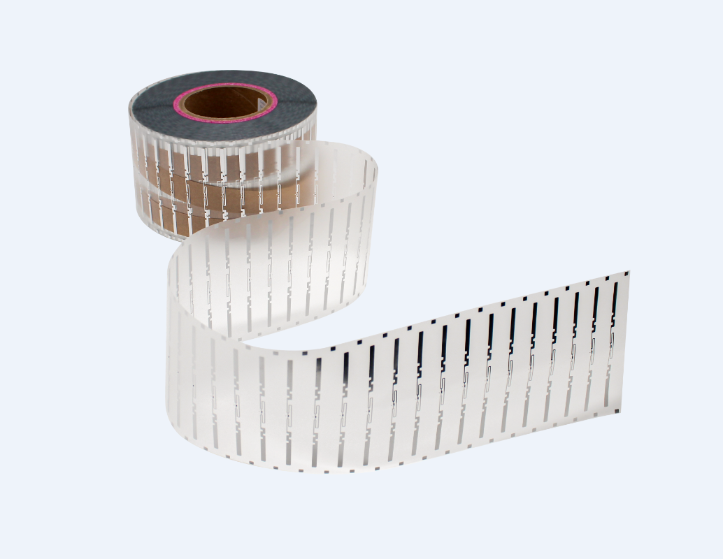
Not every gadget gets the luxury of a clean, rectangular chassis with plenty of internal breathing room. As soon as a design team starts bending curves, shrinking footprints, or wrapping electronics around a wrist, the antenna stops being a drop-in component and becomes a negotiation. Tuning in these cases isn't about hitting a single frequency on a bench—it's about coaxing acceptable performance out of an environment that was never antenna-friendly to begin with. Metal frames, dense batteries, and oddly placed display panels all conspire to detune whatever radiator you thought you had.
What often gets overlooked is how much the user's own body becomes part of the matching network. A device that sits against skin, slides into a pocket, or gets clipped to a bag sees its impedance shift constantly. You can't just tune for free space and call it done. Instead, engineers have to play with aperture tuning, impedance switching, and sometimes active components that adjust on the fly—all while keeping the bill of materials from ballooning. It's a balancing act between electrical performance, mechanical constraints, and the reality that most people won't hold their device exactly the way the datasheet assumes.
The payoff, though, is tangible. A well-tuned antenna in an unconventional form factor means fewer dropped connections, better battery life, and a device that actually works as advertised when it leaves the lab. There's no universal recipe—every oddball enclosure demands its own set of compromises. The trick is knowing which compromises hurt the least and testing them early enough that the antenna isn't an afterthought once the industrial design is locked in.
Firmware Built Around Your Product, Not the Other Way Around
Most firmware starts as a portable layer that gets bent around whatever hardware is already on the board. That leaves product teams trimming features, adding external components, or hiding timing issues in application code. Here, the low-level code is written after the schematic is finalized, not before. Power sequencing, pin muxing, clock trees, and peripheral timing are mapped directly to the silicon you actually placed.
That changes how edge cases get handled. A sensor with an awkward reset pulse, a flash chip that needs a longer write settle, a buck converter with a specific soft-start window — these aren't discovered during bring-up. The firmware already accounts for them because it was built against your bill of materials and your board layout.
The result is a device that wakes predictably, sleeps within target, and doesn't need register hacks scattered across the application. Your product works the way it was designed to, without asking the hardware to meet generic firmware halfway.
Keeping Tap Response Fast Without Killing Battery Life
Modern touchscreens face a built-in tension: users expect instant reactions, yet every millisecond of reduced latency typically demands more power. The common fix of cranking up the touch sampling rate to 240Hz or higher does make taps feel snappier, but it also keeps the digitizer and related circuitry in a near-constant high-alert state. A smarter approach involves separating the 'listen' phase from the 'process' phase. Instead of polling the screen at maximum frequency at all times, the system can idle at a modest 60Hz while waiting for any finger contact, then instantly ramp to 240Hz only for the brief duration of an active gesture. This means the screen remains responsive when it matters but drops back to a low-power idle within a few hundred milliseconds after the finger lifts off, clawing back significant battery capacity without any perceptible lag.
Another overlooked lever is offloading touch event handling to a dedicated low-power co-processor. Rather than waking the main application processor for every coordinate update, a tiny always-on microcontroller can filter raw touch data, debounce taps, and even recognize simple gestures like double-taps or long-presses. The main CPU stays in a deep sleep state until a validated gesture or a significant movement triggers a wake-up. This hardware partitioning works especially well for always-on displays and quick settings toggles, where a full system resume would be overkill. Pair this with adaptive scan rates that learn from user behavior—switching to a slower scan while reading an e-book, then back to fast response when typing—and the battery savings stack up quickly.
The payoff shows up in real-world numbers: a device that previously burned through 12-15% of its battery per hour during active touch use can drop to 7-8% with adaptive sampling and co-processor offloading, all while keeping tap-to-launch times under 80 milliseconds. That is the kind of invisible optimization users notice not as a feature, but as a phone that simply lasts longer between charges and still reacts the moment their thumb lands on the screen.
Certification Paths That Don't Eat Your Launch Window
Launch windows are unforgiving. Miss one, and you're sitting on the pad for weeks while your competitors fly overhead. The smartest teams treat certification not as a separate hurdle but as a parallel track that starts on day one. By interleaving test articles with flight hardware builds, you can shave months off the schedule without burning extra cash. The key is to stop treating paperwork as a phase-gate that happens after engineering — instead, fold it into every design review so the cert package writes itself.
There’s a quiet trick used by teams that regularly hit their dates: they pre-qualify components at the subassembly level long before the full vehicle exists. Instead of waiting for a completed launch vehicle to begin vibration and thermal cycling, they run those profiles on the avionics box, the valve stack, the ordnance chain — each on its own timetable. That way, when the integrated stack finally rolls out, the certification evidence is already in the drawer. You stop discovering problems at the eleventh hour because those problems already got solved in a lab months earlier.
And what about the dreaded review board? Most delays don’t come from the technical work — they come from waiting on signatures and rework loops. Build your cert plan backwards from the intended launch date, then pad every interface with a human being, not just a document. A walking, talking engineer who owns a specific requirement can clear a blocker in a hallway conversation. A shared spreadsheet can’t. When certification paths are designed with the same systems thinking as the vehicle itself, they quit eating your launch window and start eating the risk instead.
From CAD to First Successful Tap in Record Time
Getting from a CAD model to the first verified thread usually involves a frustrating loop of tweaks, tool changes, and test holes. But when the geometry is clean and the toolpath strategy respects the material, the tap can engage exactly as designed on the very first try. The real time savings come from eliminating the back-and-forth between the CAM station and the machine—no last-minute feed adjustments, no swapping to a different tap mid-job because the hole ended up undersized.
A big part of hitting that record pace is treating the CAD model as the single source of truth. If the hole diameters, chamfer angles, and thread depths are all locked in the file, the CAM setup becomes a formality rather than a guessing game. Pair that with a tap that matches the material’s chip behavior, and the whole process feels almost uneventful. The first hole cuts clean, the gauge goes in smoothly, and the machine keeps moving.
In practice, this means spending a few extra minutes up front verifying the model against the actual stock and tool inventory. That check prevents the kind of small errors that turn a quick tapping job into a half-day of troubleshooting. When the first tap succeeds without a single correction, the timeline from digital file to finished part shrinks dramatically—and the shop floor notice the difference.
FAQ
Off-the-shelf modules force you to design around their constraints. An ODM approach starts with your product's physical layout, battery budget, and user flow, then builds the NFC subsystem to match. The result is often a smaller footprint and fewer compromises in industrial design.
Antenna matching is the part most designs get wrong. We run co-simulation with your mechanical team early, adjust the matching network for the actual enclosure and nearby metal, and provide a tuning fixture so production units stay within spec.
Yes, the firmware is structured as a small RTOS task that can switch between reader/writer, card emulation, and peer-to-peer modes dynamically. This is useful for devices that need to read tags during setup but act as a card for access control later.
In standby with passive polling, current draw can stay in the low microamp range, depending on polling interval. Active transactions spike briefly, so the average consumption is usually dominated by how often the device wakes up, not the NFC radio itself.
We can integrate a certified secure element or use the host MCU's trusted execution environment for key storage. For lower-risk applications, a lightweight challenge-response protocol with unique per-device keys is often enough to prevent cloning.
A first prototype usually takes 6 to 10 weeks if the mechanical design is stable. That includes schematic, layout, antenna tuning, and firmware bring-up. Certification and production tooling add more time, but we can often run those in parallel.
We design with pre-certified NFC controllers and provide test guidance, pre-scan results, and documentation packages. Most clients pass FCC, CE, and NFC Forum certification on the first or second attempt without needing to re-spin the board.
Yes, a common pattern is to use an NFC tap to exchange Bluetooth pairing credentials or Wi-Fi provisioning data. This avoids typing passwords on small screens and reduces support calls for connected devices.
Conclusion
Standard NFC modules often fail when a product's industrial design pushes beyond conventional shapes and materials. Off-the-shelf antennas and firmware assume predictable layouts, leaving custom gear with poor read range or unreliable tap points. An ODM NFC solution starts from the physical realities of your device: antenna traces are tuned to match unusual enclosures, metal components, and tight internal spacing, while firmware is stripped of generic features and rewritten around the exact use case—whether it's a wearable, a smart lock, or a medical instrument. This approach removes the friction of adapting a finished module to a design it was never meant to fit.
The result is not just better connectivity but a faster path to production. Engineering teams move directly from CAD files to a first successful tap because antenna matching, power management, and protocol handling are developed in parallel with the product itself. Tap response stays quick without draining the battery, thanks to low-power polling and wake-on-field logic tuned for your specific duty cycle. Certification is handled by experts who know how to schedule pre-compliance and final testing so the launch window remains intact. Instead of forcing your device into a generic NFC template, the ODM process aligns the radio, firmware, and certification flow with how your product actually works in the real world.
Contact Us
Contact Person: Esme Mo
Email: [email protected]
Tel/WhatsApp: 0086 191 2931 7837
Website: https://www.osrfidglobal.com/